

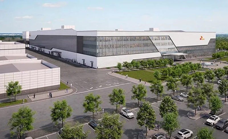
The Indiana site will package and test high-bandwidth memory chips used in AI systems.
Hanmi Global, headquartered in Seoul, South Korea, has been selected as construction manager for a planned $4-billion AI memory manufacturing facility being built by chipmaker SK hynix on 133 acres in West Lafayette, Ind., reflecting the need for a global AI memory supply to meet the technology’s rapid surge.
The project is a high-bandwidth memory (HBM) packaging plant—part of the AI semiconductor supply chain—with construction already underway and a cleanroom targeted for completion in October 2028. Hanmi Global, which handled preconstruction in 2024, will oversee the full scope of project management, including design, cost, schedule, quality, safety and coordination of U.S. and Korean partners.
The facility requires complex infrastructure—cleanrooms, power, water and gas systems—tightly synchronized with equipment installation, making integrated project management critical, Hamni Global said in a press release.
The project is SK hynix’s first AI memory production hub in the U.S. It will house an HBM production line and the Advanced Packaging R&D Testbed. SK hynix says it plans to supply next-generation HBM that has undergone on-site packaging and testing to its U.S. customers starting in the second half of 2029.
HBM is a high-value, high-performance memory product that vertically connects multiple DRAM chips to increase capacity and significantly improve data processing speeds. HBM has evolved through six generations.
Advanced packaging is an advanced semiconductor back-end process technology that overcomes the limits of fine-grained scaling to reduce chip size by integrating multiple chips into a single package or stacking them vertically to enhance performance, Sk hynix says.
Additionally, SK hynix has signed a memorandum of understanding with Purdue University for research and development in advanced packaging. They will collaborate in various areas, including joint research and talent development for next-generation AI memory.
“With Indiana serving as the home of this historic project, we hope this investment will drive new growth in the region and generate an impact that extends across the United States,” Indiana Gov. Mike Braun said at the groundbreaking.
Purdue University President Mitch Daniels said he hopes the project will be the “starting point for establishing Indiana as a hub for the semi-conductor industry and related technologies.”
In 2024, the U.S. Department of Commerce awarded SK hynix up to $458 million in direct funding under the CHIPS Incentives Program’s Funding Opportunity for Commercial Fabrication Facilities. The CHIPS Program Office is also providing up to $500 million in loans, part of the $75-billion loan authority provided by the CHIPS Act.